Catastrophic IGBT failure reasons
Facing the catastrophic fails on IGBT only at High temp i.e. 50 Deg. The pair works fine at normal temps of 26 Deg.Invite to share the reasons for probable causes. The gate drive & collector currents are within limits Frequency 22.3Khz IGBT type IRG4PH40UD2 (24Amps1200V) Used in half bridge combination & currents are 12amps peak +6amps ripple current, shared by 2 parallel devices each. Worst dv/dt is 100nS @800V.
The fails are noticed at both places in one case at intrinsic diode & full die including C-E in another device. The gate resistors are separate for both devices driven by same driver, I am under impression that -ve tempco can not be //ed but checking on this point. Is there more info on use of " sensitive magneto-thermic switch protection between the grid and the inverter (Z curve)".
The gate drive is measured with differential probe, The drive IC is supplied with +15 V & -6 V so drives measure same except worst of +11V & -3 V at + VE & -VE peaks of sine wave. The Vc-e is 800V including spikes (limited by snubbers)@750 V bus, but the diode Trr is under suspect. (I suppose there is no remedy on this except to change to new device. Is there any measure to reduce the Trr or diode current? The dead time increase (from 1.4 uS to 1.8 Us ) didn't gave relief.
From my experiences with IGBT measurements at 800V, differential probe measurements are worthless regarding wave shape. Although IGBTs are not the fastest switch elements, differential voltage probes are low bandwidth and have considerable feed through of common mode signals at higher frequencies. Further they pick up a lot of magnetic field due to the large loop between pos and neg connections. The right way to go is to use two probes connected to two osc. channels with ground connection to the same silent ground. Let the oscilloscope calculate the difference. To do this at 800V, you have to use 12 bit oscilloscope (8-bits give a discretization of >3V!) The best is to also use a calibrated probe pair, e.g. LeCroy DXC-5100.
If the diodes are still carrying current when you switch on the IGBTs, dI/dt might become larger than in normal operation, thereby adding or subtracting large voltage spikes to your circuit. 1000A/us in 10nH gives 10Vp. I have seen >20Vp over the 5mm source pin of a D2Pak MOSFET. On the other hand, if the gate resistor is directly in series with the gate (and close to it), the G-E input cap inside the device will take some time to charge or discharge, so maybe this comment is irrelevant.
There are plenty of IGBT's w/o incorporated diode. Actually the diode chip is added by manufacturer. for helping applications but I think that the best is to select each component separately. I had the same problem you describe in designing an 5kw inverter and finally by changing a Fairchild soft recovery diode with Si-C diode (you also can parallel them as mosfets) I get rid of any snubber and increased much the efficiency, but mostly it worked pretty cold. The same problem appears in boost converters (like PFC) and the same H.V schottky diode solves the problem.
For curiosity, some 15 years ago Motorola developed a special diode MURH860 with a special technology which was the only one working in PFC circuits without special complex snubbers (L-C-R-D). I am sure a lot of people remembers it.
The site has great info. I have been working with igbts for a couple of months now. what i've noticed is, they are quite sensitive and should be shielded carefully.
Post a Comment:
You may also like:

Power Inverter Source
Featured Articles
How to Choose a Suitable Power ...
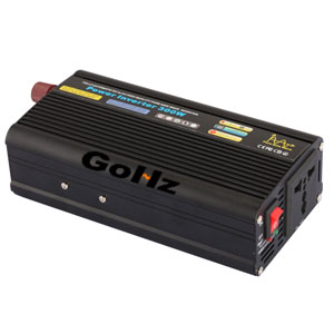 How to select the inverter for an air conditioner, television, computer or the motor? How to match the battery? How long is the ...
 How to select the inverter for an air conditioner, television, computer or the motor? How to match the battery? How long is the ...
12V 300W Uni-polar Isolation Pure Sine ...
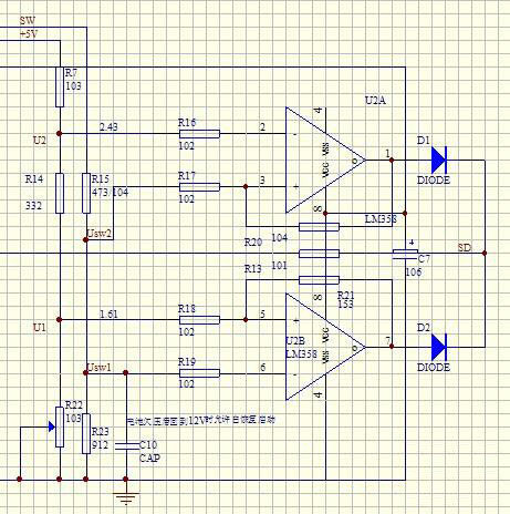 12v 300w uni-polar isolation of pure sine wave inverter Basic parameters Nominal power: 300W; continuous power: 250W; Peak power: ...
 12v 300w uni-polar isolation of pure sine wave inverter Basic parameters Nominal power: 300W; continuous power: 250W; Peak power: ...
600w Pure Sine Wave Power Inverter ...
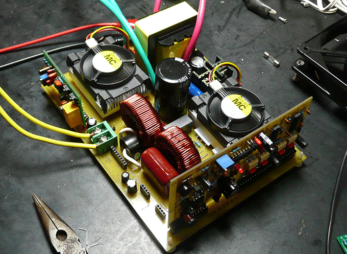 I spent nearly a month design a 600w pure sine wave power inverter. The machine has the following characteristics: 1. SPWM drive ...
 I spent nearly a month design a 600w pure sine wave power inverter. The machine has the following characteristics: 1. SPWM drive ...
1000w 12V DC Home Power Inverter ...
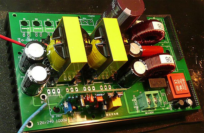 This power inverter is designed for 12v DC, but also can be connected to 24v DC, my goal is 800 watt, strive to 1000 watt pure ...
 This power inverter is designed for 12v DC, but also can be connected to 24v DC, my goal is 800 watt, strive to 1000 watt pure ...